Alain C. Diebold
Ph.D.

Professor Emeritus, Empire Innovation Professor of Nanoscale Science
Faculty/Staff
Faculty
Department
Nanoscience
College
College of Nanoscale Science + Engineering
Nanoscale Science Dr. Alain Diebold
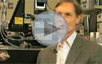
Watch Professor Diebold's "Inside CNSE" video interview on metrology.
Degrees
- Ph.D., Statistical Mechanics of Gas-Solid Surface Scattering, Purdue University, 1979
- B.S., Chemistry, Indiana University-Purdue University, 1975
Areas of Research
- Nanoscale metrology and materials science
- Materials characterization at the nanoscale
- Semiconductor metrology and characterization
Awards
- SPIE Fellow
- AVS Fellow
Description of Research
The main focus of Professor Diebold's research will be in the area of nanoscale metrology and materials science. Research interests include the materials properties and measurement of future materials and structures such as nanowire FETs and ferroelectric High K as well as 2D and topological materials. Measurement of nanoscale films and structures requires a thorough understanding of the role of uniquely nanoscale phenomena on the properties of nanoscale semiconductors and metals. In that light, the group uses a variety of characterization and metrology methods including near IR, visible, and UV optical methods such as ellipsometry and second harmonic generation as well as X-Ray methods. Synchrotron X-Ray characterization has proven essential to characterization of ultra-thin films. Another research area is the imaging and characterization of nano-scale structures using electron microscopy. Simulation of transmission electron microscopy (TEM) and scanning TEM (STEM) imaging is more important than ever as aberration corrected microscopes are introduced. This work will be done in collaboration with other faculty, industrial partners, and research institutions.
In the area of semiconductor metrology and characterization, Professor Diebold's industry coordination and collaborative development of new methods and technology will continue. Research in this area will include critical dimension measurement and process control.
Editorial Activity
- Associate Editor IEEE Transactions on Semiconductor Manufacturing
Conferences of Interest
ICSE 9 Beijing
9th International Conference on Spectroscopic Ellipsometry
May 22-28, 2022
http://www.icse-9.com/En/Default
Frontiers of Characterization and Metrology for Nanoelectronics – 2022
Monterey, CA March 14-17, 2022
https://fcmn2022.avs.org/
ICSE 8 Barcelona
8th International Conference on Spectroscopic Ellipsometry
May 26-31, 2019
https://congresses.icmab.es/icse8/
Frontiers of Characterization and Metrology for Nanoelectronics – 2019
Monterey, CA April 1-5, 2019
https://www.nist.gov/news-events/events/2017/03/frontiers-characterization-and-metrology-nanoelectronics
AVS 65th International Symposium & Exhibition
Long Beach, CA October 18-23, 2018
Focus Topic on Spectroscopic Ellipsometry
Focus Topic on Manufacturing Science and Technology
https://s19.a2zinc.net/clients/avs/avs18/public/enter.aspx
TOM 6 - Frontiers in Optical Metrology
Delft, Netherlands October 8-12, 2018
www.myeos.org/events/eosam2018_tom6
2017 Frontiers of Characterization and Metrology for Nanoelectronics, Monterey, CA, March 21-23, 2017 https://www.nist.gov/news-events/events/2017/03/frontiers-characterization-and-metrology-nanoelectronics
ECS SiGe, Ge, & Related Compounds: Materials, Processing, and Devices Symposium in October 2016
www.sigesymposium.org
Surface Analysis 2016, August 16-18, 2016
7th International Conference on Spectroscopic Ellipsometry (ICSE-7), June 6-10, 2016
http://www.icse-7.de/
6th International Conference on Spectroscopic Ellipsometry (ICSE-VI), May 26-31, 2013
Co-Chair of 2013 Frontiers of Characterization and Metrology for Nanoelectronics
Co-Chair 2011 33rd Symposium on Applied Surface Analysis
Conference Web Link
Chair 2010 International Conference of Spectroscopic Ellipsometry
Chair 2009 Technical Sessions of American Vacuum Society's Manufacturing Science and Technology Group
Co-Chair of 2009 Frontiers of Characterization and Metrology for Nanoelectronics
Recent Invited Presentations
Metrology for Advanced Transistor and Memristor Devices and Materials, A.C. Diebold and N. Cady, Proceedings of SPIE Advanced Lithography: Metrology, Inspection, and Process Control for Microlithography XXXIII, San Jose, Feb. 23-27, 2020.
The Application of Mueller Matrix Spectroscopic Ellipsometry to Scatterometry Measurement of Feature Dimension and Shape for Integrated Circuit Structures, 66th AVS National Symposium, Columbus, Oct. 20-25, 2019.
The application of Mueller Matrix Spectroscopic Ellipsometry based Scatterometry to determination of the feature shape and dimensions of integrated circuit structures, Invited Tutorial Talk at the International Conference on Spectroscopic Ellipsometry VIII, Barcelona, May 26 – 31, 2019.
Advances in Optical Dimensional Metrology and Microscopy, Critical Materials Conference, Saratoga, April 26, 2019.
The application of Mueller Matrix Spectroscopic Ellipsometry based Scatterometry to determination of the feature shape and dimensions of integrated circuit structures, Invited Tutorial Talk at the International Conference on Spectroscopic Ellipsometry VIII, Barcelona, May 26 – 31, 2019.
The Application of Mueller Matrix Spectroscopic Ellipsometry to Scatterometry Measurement of Feature Dimension and Shape for Integrated Circuit Structures, 66th AVS National Symposium, Columbus, Oct. 20-25, 2018.
The Application of Mueller Matrix Spectroscopic Ellipsometry to Scatterometry based Measurement of Feature Shape and Dimension, Plenary Note Talk for Frontiers in Optical Metrology, TOM6, European Optical Society Biannual Meeting 2018, Delft, Oct. 8 – 12, 2018.
Nanometrology and Nanocharacterization in Nanoelectronics, 2017 AVS National Symposium, Oct. 30 – Nov. 3, Tampa, FL.
Muller matrix-based scatterometry, 2017 International Conference on Frontiers of Characterization and Metrology for Nanoelectronics, Monterey, CA, Mar. 21-23, 2017.
Materials Characterization at the Nanoscale, UT Dallas, March 11, 2016
Semiconductor Industry Needs for Electron Microscopy, in “Electron Microscopy Frontiers: Metrology Opportunities and Challenges”, NIST, Gaithersburg, March 8 & 9, 2017.
Characterization and Metrology from FinFETS & Interconnect to Beyond CMOS materials, Semicon Korea 2016, Seoul, Korea, February Feb. 9, 2017.
Importance and Challenges of Metrology for Nanoscale Materials and Semiconductor Structures, Determining the Composition and Structure of Small Volumes II, Oregon Challenges Workshop Keynote Talk, Eugene, July 28 and 29, 2015.
Synchrotron Metrology for Ultra-Thin Films Deposited by ALD for Emerging MOS Devices, Sonal Dey and Alain Diebold, Workshop on Semiconductor Technology Development through Characterization by Synchrotron and Electron Microscopy Techniques at the NSLS-II/CFN Users’ Meeting, Brookhaven National Laboratory, May 20, 2015.
Optical Properties of Nanoscale Nanoelectronic Materials, University of Texas San Antonio Department of Physics, April 11, 2014.
Metrology Tools for Semiconductor Manufacturing, in the Advances in Measurement Technology Session at the March 2014 APS meeting, Denver, March 3 to 7, 2014.
Optical Properties of Nanoscale Nanoelectronic Materials, Laboratory of Surface Modification (LSM) Seminar Series, Rutgers University, Nov. 14, 2013.
Optical Properties of Nanoscale Materials, A.C. Diebold, AVS National Symposium, Long Beach, CA, October 27 - November 1, 2013.
The 2012 ITRS Metrology Roadmap, A.C. Diebold and C. Hacker, 2013 Frontiers of Characterization and Metrology for Nanoelectronics, Gaithersburg, MD, March 26 -28, 2013.
Beyond Graduate School: Academic and Industrial Science, Center for Nanohybrid Function Materials NSF-EPSCoR Symposium, University of Nebraska, Oct. 15, 2012.
Metrology for Advanced Gate Dielectric Materials, Synchrotron Techniques in Microelectronics Research at the 2012 NSLS/CFN Joint Users' Meeting, Brookhaven National Laboratory, May 23, 2012.
The Effect of Electron Phonon Interactions on Optical Properties of Nanoscale Films, European Materials Research Society (E-MRS), Strasbourg, May 14-18, 2012.
Characterization and Metrology Roadmap for Future CMOS, Frontiers of Characterization and Metrology for Nanoelectronics 2011, May 23 - 27, 2011.
Semiconductor Metrology from New Transistor and Interconnect Materials to Future Nano-Structures; Keynote talk as a part of the “opening ceremonies” for Metrology, Inspection, and Process Control for Microlithography XXV, at SPIE Advanced Lithography, San Jose, 27 February - 4 March 2011.
Topic Optical Characterization of Graphene, Physical Chemistry Seminar, Department of Chemistry, Purdue University, March 2, 2011.
Optical Characterization of CVD Graphene using Spectroscopic Ellipsometry, University of Delaware, Materials Science seminar, Oct. 13, 2010.
3D Integration: Processes, Materials and Analysis (with Ehrenfried Zschech, Fraunhofer IZFP Dresden), at the 3D Interconnect Process Control and Quality Engineering Tutorial at the Electronics System Integration Technology Conferences 2010, September 13, 2010. Berlin, Germany
Optical spectroscopy for bonded wafer inspection: IR, Raman at the 3D Interconnect Process Control and Quality Engineering Tutorial at the Electronics System Integration Technology Conferences 2010, September 13, 2010. Berlin, Germany
Graphene Characterization and Metrology and its Standardization, Fourth International Workshop on Metrology, Standardization and Industrial Quality of Nanotubes (MSIN10), Montreal, 27 June 2010.
From the Lab to the FAB: the Progression of Laboratory to FAB based Measurements, 10th European Advanced Equipment Control/Advanced Process Control (AEC/APC) Conference, Catania, Sicily - Italy, April 21 - 23, 2010.
Metrology of Advanced Materials with Emphasis on High K - Metal Gate and Graphene, KLA-Tencor's CTO Seminar Series, July 16, 2009.
Process integration and process characterization of high-k/metal gate stacks, 18th Material for Advanced Metallization Workshop, Grenoble, France, March 8 to 11, 2009.
Overview of Optical Measurements for Advanced Transistor Processes, Columbia University, Dec. 9, 2008.
Impact of Quantum Confinement on the characterization of thin semiconductor films, AVS - Surface Analysis 2008, State College, PA, June 2008
Metrology requirements for double patterning - Approaching the Optical Limit: Practical Methods for Patterning 22nm HP and Beyond, Lake George, NY, May 15, 2008
Are Optical Measurements Sensitive to Quantum Confinement?, DPG 2008 Annual Meeting of the German Society of Physics (DPG), Berlin, Feb 25-29, 2008
Optical Characterization of Thin Semiconductor and Metal Films, FENA ONAMI Workshop on Nanoelectronics for High Performance Computing and Information Processing, UCLA, Nov. 20, 2007
Optical Observation of Quantum Confinement and Quantum Size Effects, Rutgers Surface Science Seminar Series, Sept. 13, 2007
Ellipsometry and NanoMetrology, 4th International Conference on Spectroscopic Ellipsometry, Stockholm, June 11-15, 2007
Metrology for Nanoelectronics: Metrology Roadmap, AEC-APC Europe, Dresden, April 17-19, 2007
Characterization and Metrology for Nanoelectronics, Frontiers of Characterization and Metrology for Nanoelectronics, Gaithersburg, March 27-29, 2007
Metrology for Nanoelectronics: the Impact of Nanoscale Dimensions, Workshop on Metrology for Beyond CMOS, FENA, San Francisco, Dec. 14, 2006
Characterization and Metrology for Nanoelectronics, Albany NanoTech, Oct. 31, 2006
Characterization and Metrology for Nanoelectronics, NIST Center for Nanoscale Science and Engineering Seminar Series, Oct. 16, 2006
Metrology at the Leading Edge, IEEE Engineering Management Conference, University of Texas, Aug. 10, 2006
Impact of Nanosized Dimensions on Characterization and Metrology, IBM Yorktown Heights, May 5, 2006
Metrology for Nanoelectronics: Future Needs and the Transition of Lab Methods into the FAB, Fraunhofer Center for Nanoelectronics, Dresden, April 5, 2006
Metrology (including Materials Characterization) for Nanoelectronics, SPIE Conference on Testing, Reliability, and Application of Micro- and Nano-Materials Systems IV, San Diego, 26 Feb - Mar. 2, 2006
The importance of aberration corrected SEM and TEM to the Semiconductor Industry, November, 2005, 52nd National Symposium of the AVS, Boston, MA
Characterization for Next Generation Semiconductor Process Development by Analytical Electron Microscopy, Brendan Foran, Mark Clark, Guoda Lian, Michael Campin, & Alain Diebold, ECASIA, September, 2005
Interface Sensitive Measurement of High k Film Stacks using Optical Second Harmonic Generation, American Physical Society Meeting, March 2005
Metrology for Nanoelectronics, Characterization and Metrology for ULSI Technology, March 2005
Significant Books
- Optical and Electrical Properties of Nanoscale Materials, Alain C. Diebold and Tino Hofmann, (Springer Nature, 2021).
- Handbook of Silicon Semiconductor Metrology (Dekker, 2001)
Co-editor of
- Frontiers of Metrology and Characterization for Nanoelectronics (2007 & 2009), AIP Press.
- Characterization and Metrology for ULSI Technology (1998, 2000, 2003, and 2005), AIP Press.
- Semiconductor Characterization: Present Status and Future Needs (1996).
- Analytical and Diagnostic Techniques for Semiconductor Materials, Devices, and Processes 7, ECS Transactions Vol. II No. 3 2007.
Recent Publications
Optical Properties: 2D and Topological Materials
Optical second harmonic generation from silicon (100) crystals with process tailored surface and embedded silver nanostructures for silicon nonlinear nanophotonics, Bhowmik, Y.Q. An, S. Schujman, A.C. Diebold, and M. Huang, J. Appl. Phys. 128, (2020) 165106.
High K- Metal Gate and Interconnect Barrier Characterization
- Ferroelectric phase in 7 nm Hf(1-x)ZrxO2 thin films, V. Mukundan, S.M. Consiglio, D.H Triyoso, K. Tapily, M.E McBriarty, S. Schujman, K. Beckmann, V. Kaushik, N. Cady, R. Clark, G. Leusink, A.C. Diebold, submitted.
- Quantifying non-centrosymmetric orthorhombic phase fraction in 10 nm ferroelectric Hf0.5Zr0.5O2 thin films, V. Mukundan, S. Consiglio, D.H. Triyoso, K. Tapily, S. Schujman, C. Mart, T. Kämpfe, W. Weinreich, R.D. Clark, G.J. Leusink, and A.C. Diebold, Appl. Phys. Lett. 117, (2020), 262905.
Quantifying non-centrosymmetric orthorhombic phase fraction in 10 nm ferroelectric Hf0.5Zr0.5O2 thin films, V. Mukundan, S. Consiglio, D.H. Triyoso, K. Tapily, S. Schujman, C. Mart, T. Kämpfe, W. Weinreich, R.D. Clark, G.J. Leusink, and A.C. Diebold, submitted.
Characterization of nanoscale sub-surface features during selective etching of multi-layered Nanowire Test Structures using Critical Dimension – Small Angle X-Ray Scattering, M. Korde, S. Kal, C. Alix, A. Mosden, R.J. Kline, D. Sunday, and A.C. Diebold in preparation.
Non-destructive characterization of nanoscale sub-surface features during selective etching of multi-layered Nanowire Test Structures using Mueller Matrix Spectroscopic Ellipsometry based scatterometry, M. Korde, S. Kal, C. Alix, N. Keller, G.A. Antonelli, A. Mosden, A.C. Diebold, J. Vac. Sci. Technol. B, 38, (2020), 024007.
Metrology of nanowire / nanosheet FETs for advanced technology nodes, M. Korde, R. J. Kline, D.F. Sunday, N. Keller, S. Kal, C. Alix, A. Mosden, A.C. Diebold, Proceedings of SPIE Advanced Lithography: Metrology, Inspection, and Process Control for Microlithography XXXIII, San Jose, Feb. 23-27, 2020.
Optical Characterization of multi-NST Nanowire Test Structures using Muller Matrix Spectroscopic Ellipsometry (MMSE) based scatterometry for sub 5nm nodes, M. Korde, S. Kal, C. Pereira, N. Keller, A. Mosden, and A.C. Diebold, Proceedings of SPIE Advanced Lithography: Metrology, Inspection, and Process Control for Microlithography XXXIII, San Jose, Feb. 24-28, 2019. Proc. of SPIE Vol. 10959 109590X.
Structural correlation of ferroelectric behavior in mixed hafnia-zirconia high-k dielectrics for FeRAM and NCFET applications, V. Mukundan, K. Beckmann, K. Tapily, S. Consiglio, R. Clark, G. Leusink, N. Cady, A.C. Diebold, MRS Advances (2019), pp 1-17. https://doi.org/10.1557/adv.2019.148
Fermi level manipulation through native doping in the topological insulator Bi2Se3, L.A. Walsh, A.J. Green, R. Addou, W. Nolting, C.R. Cormier, A.T. Barton, T.R. Mowll, R. Yue, N. Lu, N. Kim, M.J. Kim, V.P. LaBella, C. Ventrice, S. McDonnell, W.G. Vandenberghe, R.M. Wallace, A.C. Diebold, and C.L. Hinkle, ACS Nano 12, (2018), pp 6310-6318. online DOI: 10.1021/acsnano.8b03414.
Perspective: Optical measurement of feature dimensions and shapes by scatterometry, A.C. Diebold, A. Antonelli, N. Keller, APL Mat. 6, (2018), 058201, https://aip.scitation.org/doi/10.1063/1.5018310
Transiently stimulated second-harmonic generation from silicon nanogratings, Y.Q. An and A.C. Diebold, Phys. Rev. B 96, (2017), 201306R.
Atomic layer deposited ultra-thin metal nitride barrier layers for ruthenium interconnect applications, S. Dey, K-H Yu, S. Consiglio, K. Tapily, T. Hakamata, C.S. Wajda, and G.J. Leusink, J. Jordan-Sweet, C. Lavoie, D. Muir and B. Moreno, and A.C. Diebold, J. Vac. Sci. Technol. A35, (2017), 03E109.
Role of Ge and Si substrates in higher-k tetragonal phase formation and interfacial properties in cyclical ALD-anneal Hf1-xZrxO2/Al2O3 thin film stacks, S. Dey, K. Tapily, S. Consiglio, R. D. Clark, C. S. Wajda, G. J. Leusink, A.R. Woll, and A.C. Diebold, J. Appl. Phys. 120, (2016), 125304.
Surface Oxidation of the Topological Insulator Bi2Se3, A.J. Green, S. Dey, Y.Q. An, B. O’Brien, S. J. O’Mullane, B. Thiel, and A.C. Diebold, J. Vac. Sci. Technol. A34, (2016), 061403.
Utilizing Tunable Absorption Properties of Light for Enhanced Ellipsometry of Metal Gratings, S. O’Mullane, Nick Keller, J. Race, A.C. Diebold, Journal of Micro/Nano Lithography, MEMS & MOEMS 15, (2016), 044003.
Tracking quintuple layer oxidation on cleaved Bi2Se3 by optical second-harmonic anisotropy, Y. An, A.J. Green, and A.C. Diebold, Phys. Rev. B. 93, (2016), 241308(R).
Optical CD Metrology for Directed Self-Assembly Assisted Contact Hole Shrink,D.J. Dixit, A. Green, E.R. Hosler, V. Kamineni, M. Preil, N. Keller, J. Race, J.S. Chun, M. O’Sullivan , P. Khare, W. Montgomery, A.C. Diebold, Journal of Micro/Nano Lithography, MEMS & MOEMS 15(1), (2016), 014004.
Pulsed-N2 assisted growth of 5-20 nm thick β- W films, A. Narasimham, A. Greene, R. Matyi, P. Khare, T. Vo, A.C. Diebold, and V. LaBella, AIP Advances 5, (2015), 117107.
Metrology for Block Copolymer Directed Self-Assembly Structures using Mueller matrix based Scatterometry, D. J. Dixit, V. Kamineni, R. Farrell,, E. R. Hosler,, M. Preil, J. Race, B. Peterson, A. C. Diebold, Control of IC Patterning Variance. Part 1: Metrology, Process Monitoring, and Control of Critical Dimension in Journal of Micro/Nano Lithography, MEMS & MOEMS 14, (2015), 021102-0 21102.
Electrical Enhancement and Higher-K Engineering in Ultra-Thin Atomic Layer Deposited Hf1-xAlxOy Films, K. Tapily, S. Consiglio, R. D. Clark, R. Vasic, C. S. Wajda, J. Jordan-Sweet, G. J. Leusink, and A.C. Diebold, ECS Journal of Solid State Science and Technology, 4, (2015), N1-N5.
Enhancing One Dimensional Sensitivity with Plasmonic Coupling, S. O’Mullane, B. Peterson, J. Race, N. Keller, A.C. Diebold, Optics Express 22, (2014), 26247.
The optical properties of pseudomorphic Ge(1-x)Snx (x = 0 to 0.11) alloys on Ge(001), M. Medikonda, G. R. Muthinti, R. Vasic, T. Adam, A. Reznicek, M. Wormington, G. Malladi and A.C. Diebold, J. Vac. Sci. Technol. B 32, (2014) 061805 (2014).
Thickness and Rotational Effects in Simulated HRTEM Images of Graphene on Hexagonal Boron Nitride, A. J. Green and A.C. Diebold, Microscopy and Microanalysis 20, (2014), 1753-1763.
High-energy “plasmons” in graphene are not plasmons, F. J. Nelson, J.-C. Idrobo, J. Fite, Z. L. Mišković, S.J. Pennycook, S.T. Pantelides, J.U. Lee, and A.C. Diebold, Nano Letters, 14, (2014), pp 3827-3831.
Engineering crystallinity of atomic layer deposited gate stacks containing HfO2 and a Ti-based metal gate: Effects of post metal gate anneal and integration schemes, S. Consiglio, K. Tapily, R.D. Clark, T. Hasegawa, F. Amano, G.J. Leusink, J. Jordan-Sweet, R. Vasić, M. Medikonda, and A.C. Diebold, J. Vac. Sci. Technol. B, (2014), J. Vac. Sci. Technol. B 32(3), (2014), 03D122.
Enhanced optical second-harmonic generation from current-biased graphene on the substrates of Si and SiC, Y.Q. An, J.E. Rowe, , D.B. Dougherty, J.U. Lee, and A.C. Diebold, Phys. Rev. B 89, (2014), 115310.
Measurement of Periodicity and Strain in Arrays of Single Crystal Silicon and Pseudomorphic Si1-xGex/Si Fin Structures using X-ray Reciprocal Space Maps, M. Medikonda, G. Muthinti, J. Fronheiser, V. Kamineni, M. Wormington, K. Matney, T. Adam, E. Karapetrova and A.C. Diebold, J. Vac. Sci. Technol. B32, (2014), 021804.
Enhanced optical second-harmonic generation from current-biased graphene on a SiO2/Si(001) substrate, Y.Q. An, F.J. Nelson, J.U. Lee, and A.C. Diebold, Nano Lett., 13, (2013), 2104.
Multi-technique X-Ray and Optical characterization of crystalline phase, texture and electronic structure of atomic layer deposited HfxZr1-xO2 gate dielectrics deposited by a cyclical deposition and annealing scheme, R. Vasić, S. Consiglio, R.D. Clark, K. Tapily, M. Medikonda, G.R. Muthinti, E. Bersch, J.J. Sweet, C. Lavoie, G. J. Leusink, and A.C. Diebold, J. Appl. Phys. 113, (2013), 234101.
Characterization of E-beam patterned grating structures using Mueller Matrix based Scatterometry, G.R. Muthinti, B. Peterson, R.K. Bonama and A.C. Diebold, Journal of Micro/Nano Lithography, MEMS & MOEMS 12, (2013), 013018.
Texturing and Tetragonal Phase Stabilization of ALD HfxZr1-xO2 using a Cyclical Deposition and Annealing Scheme, K. Tapily, S. Consiglio, R. D. Clark, R. Vasic, E. Bersch, I. Wells, J. Jordan-Sweet, G. J. Leusink, and A.C. Diebold, ECS Trans. 45, (2012), p 411.
Effects of stress on the dielectric function of strained pseudomorphic Si1-xGex alloys from 0 to 75 % Ge grown on Si (001) G.R. Muthinti, M. Medikonda, T.N. Adam, A. Reznicek, and A.C. Diebold, J. Appl. Phys. 112, (2012), 053519.
Optical and structural characterization of epitaxial graphene on vicinal 6H-SiC(0001)–Si by spectroscopic ellipsometry, Auger spectroscopy, and STM, F. Nelson, A. Sandin, D.B. Dougherty, D.E. Aspnes, J.E. Rowe, and A.C. Diebold, J. Vac. Sci. Technol. B 30, (2012), 04E106.
Cross characterization of ultra thin interlayers in HfO2 high-k stacks by ARXPS, MEIS and GIXUVR, M. Banyay, L. Juschkin, D. França, E. J. Bersch 3, A.C. Diebold, M. Liehr J. Vac. Sci. Technol. A, (2012), 041506.
Crystallinity of Electrically Scaled Atomic Layer Deposited HfO2 from a Cyclical Deposition and Annealing Scheme, S. Consiglio, R. D. Clark, E. Bersch, J. D. LaRose, I. Wells, K. Tapily, G. J. Leusink, and A. C. Diebold, J. Electro. Chem. Soc., 159, (2012), G80-G88.
Optical and structural characterization of thermal oxidation effects of erbium thin films deposited by electron beam on silicon, H.S. Kamineni, V.K. Kamineni, R.L. Moore II, S. Gallis, A.C. Diebold, M. Huang, and A.E. Kaloyeros, J. Appl. Phys. 111, (2012), 013104.
Electron-phonon interaction effects on the direct gap transitions of nanoscale Si films, V.K. Kamineni and A.C. Diebold, Appl. Phys. Lett. 99, (2011), 151903. http://apl.aip.org/resource/1/applab/v99/i15/p151903_s1
Formation of optical barriers with excellent thermal stability in single-crystal sapphire by hydrogen ion implantation and thermal annealing, W. Spratt, M. Huang, C. Jia, L. Wang, V.K. Kamineni, A.C. Diebold, and H. Xia, 99, (2011), 111909. http://apl.aip.org/resource/1/applab/v99/i11/p111909_s1
Applying X-ray Microscopy and Finite Element Modeling to Identify The Mechanism of Stress-Assisted Void Growth In Through Silicon Via (TSV), L.W. Kong, J. Lloyd, K. B Yeap, E. Zschech, A. Rudack, and A.C. Diebold, J. Appl. Phys. 110, (2011), 053502 1-7. http://jap.aip.org/resource/1/japiau/v110/i5/p053502_s1
Structural Characteristics of Electrically Scaled ALD HfO2 from Cyclical Deposition and Annealing Scheme, S. Consiglio, R. D. Clark, E. Bersch, J. D. LaRose, I. Wells, K. Tapily, G. J. Leusink, and A.C. Diebold, ECS Transactions 41 (2), (2011) pp. 89-108. http://www.ecsdl.org/getabs/servlet/GetabsServlet?prog=normal&id=ECSTF8000041000002000089000001&idtype=cvips&gifs=yes&ref=no
Effect of the interfacial SiO2 layer on the flatband voltage of TiN/HfO2/SiO2/p-Si stacks with and without La2O3 Vt-shift layers, E. Bersch, M. Di, S. Consiglio, R.D. Clark, G.J. Leusink, and A.C. Diebold, submitted.
Determination of the band gaps of ultrathin HfO2 films using spectroscopic ellipsometry, M. Di, E. Bersch, S. Consiglio, R.D. Clark, and G.J. Leusink, T. Kaack, and A.C. Diebold, J. Vac. Sci. Technol. A 29, (2011), 041001-1 to 8.
Investigation of optical properties of BCB wafer bonding layer used for 3D-Interconnects via Infrared Spectroscopic Ellipsometry, V. K. Kamineni, P. Singh, L.-W. Kong, J. Hudnall, J. Qureshi, C. Taylor, A. Rudack, S. Arkalgud, and A.C. Diebold, Thin Solid Films, 519(2011) 2924–2928.
Dielectric properties and thickness metrology of strain engineered GaN/AlN/Si(111) thin films grown by MOCVD, M. Tungare, V. K. Kamineni, A.C. Diebold, F. Shahedipour-Sandvik, Thin Solid Films, 519 (2011) 2929–2932.
Extension of Far UV spectroscopic ellipsometry studies of High-k dielectric films to 130 nm, V. K. Kamineni, J. Hilfiker, J. Freeouf, J. Fielden, S. Consiglio, R. Clark, G.J. Leusink, and A.C. Diebold, Thin Solid Films, 519 (2011) 2894–2898.
Spectroscopic Ellipsometry Characterization of High-k Metal Gate Stacks with Vt Shift Layers, M. Di, E. Bersch, S. Consiglio R. Clark, T. Zhang, P. Tyagi, Gert Leusink, T. Kaack and A.C. Diebold, Thin Solid Films, 519 (2011) 2889–2893.
Optical Properties of Large-Area Polycrystalline Chemical Vapor Deposited Graphene by Spectroscopic Ellipsometry, F. J. Nelson, V.K. Kamineni, T. Zhang, E. S. Comfort, J-U Lee, A.C. Diebold, Appl. Phys. Lett., 97, (2010), 253110 1-3.. Selected for the January 3, 2011 issue of Virtual Journal of Nanoscale Science & Technology.
Systematic study of the effect of La2O3 incorporation on the flatband voltage and Si band bending in the TiN/HfO2/SiO2/p-Si stack, M. Di, E. Bersch, S. Consiglio, R.D. Clark, G.J. Leusink, and A.C. Diebold, J. Appl. Phys., 108, (2010), 114107 1-7.
Optical Metrology of Ni and NiSi thin films used in the self-aligned silicidation process, V. K. Kamineni, M. Raymond, E. J. Bersch, B. B. Doris, A.C. Diebold, J. Appl. Phys., 107, (2010), pp 093525 1-8.
Complete Band Offset Characterization of HfO2/SiO2/Si stacks, E. Bersch, M. Di, S. Consiglio, R. Clark, G. Leusink, and A.C. Diebold, J. Appl. Phys. 107, (2010) pp 043702 :1 – 13.
Simulation Study Of Aberration-Corrected High Resolution Transmission Electron Microscopy (HRTEM) Imaging Of Few-Layer-Graphene (FLG)
Stacking, F. Nelson, A.C. Diebold, and R. Hull, Microscop. & Microanal., 16, (2010), pp 194-199.
Graphene Metrology and Devices (review article), A.C. Diebold and F. Nelson, Int. Jour. Mat. Res., 101, (2010), pp 175 - 181.
Advanced Metrology for Next Generation Transistors, A.C. Diebold, Advances in Solid State Physics Vol. 48, (Springer, Berlin, 2009), pp 371-383.
Optical Properties of Semiconductors, D.G. Seiler, S. Zollner, and A.C. Diebold, and P.M. Amirtharaj In Handbook of Optics Volume IV, 3nd edition, (McGraw Hill, New York, 2009), Chapter 5.
Observation of quantum confinement and quantum size effects, A.C. Diebold and J.Price, Phys. Stat. Sol. (a) 205, No. 4, (2008), pp 896–900.
Quantum Level Metrology, Semiconductor International, August, 2009.
Identification of Sub-Bandgap Absorption Features at the High-κ / Silicon interface and Their Relation to Charge Trapping States, J. Price, H-J Li, P. Lysaght, and A.C. Diebold, Appl. Phys. Lett. 91, (2007), pp 61925-1 - 61925-3
X-Ray Reflectometry Determination of Structural Information from Atomic Layer Deposition Nanometer-scale Hafnium Oxide Thin Films D. Windover, D. L. Gil, J. P. Cline, A. Henins, N. Armstrong, P. Y. Hung, S. C. Song, R. Jammy, and A.C. Diebold, to appear in Proceedings of MRS
Application of Aberration Corrected TEM and Image Simulation to Nanoelectronics and Nanotechnology, B. Korgel, D.C. Lee, T. Hanrath, M.J. Yacamann, A. Thesen, M. Matijevic, R. Kilaas, C. Kisielowski, and A.C. Diebold, IEEE Trans. Semicon. Manufact. 19, (2006), pp 391-396
Spectroscopic Ellipsometry Characterization of Ultra-Thin Silicon-on-Insulator Films, J. Price and A.C. Diebold, J. Vac. Sci. Technol. B24, (2006), pp 2156-2159
Optical characterization of process-dependent charging in hafnium oxide structures, R. Carriles, J. Kwon, Y. Q. An, S. Stanley, J. G. Ekerdt, M. C. Downer, J. Price, and A.C. Diebold, J. Vac. Sci. Tech. B24, (2006), pp 2160-2168
Second-Harmonic Characterization of Si/Hf(1-x)SixO2 Structures, R. Carriles, J. Kwon, J. C. Miller, Y. Q. An, M. C. Downer, J. Price, and A.C. Diebold, Appl. Phys.Lett. 88, (2006), p 161120
Spatial distributions of trapping centers in HfO2/SiO2 gate stacks, D. Heh, C.D. Young, G.A. Brown, P.Y. Hung, A.C. Diebold, G. Bersuker, E.M. Vogel, and J.B. Bernstein, Appl. Phys. Lett. 88, 152907 (2006)
Optical band gaps and composition dependence of hafnium-aluminate thin films grown by atomic layer chemical vapor deposition, N. V. Nguyen, S. Sayan, I. Levin, J. R. Ehrstein, I. J. R. Baumvol and C. Driemeier, C. Krug, L. Wielunski, P. Y. Hung and Alain Diebold, J. Vac. Sci. Technol. A23, 2005, pp 1706-1713
Study of Two-Dimensional B Doping Profile in Si FinFET Structures by HAADF, D. Garcia-Gutierrez, A.A. Khajetoorians, X.D. Wang, D. Pham, H. Celio, A.C. Diebold, C.K. Shih and M. Jose-Yacaman, J. Vac. Sci. Technol. B24, 2006, pp 730-738
X-ray reflectometry and x-ray fluorescence monitoring of the atomic layer deposition process for high-k gate dielectrics, P. Y. Hung, C. Gondran, A. Ghatak-Roy, S.Terada, B. Bunday, H. Yeung, A.C. Diebold, J. Vac. Sci. Technol. B23, (2005), pp 2244-2248
Electrical Characterization of Spatial Distributions of Trapping Centers in HfO2/SiO2 Stacked Dielectrics, D. Heh, E.M. Vogel, J.B. Bernstein, C.D. Young, G.A. Brown, G. Bersuker, P.Y. Hung, and A.C. Diebold, submitted to IEEE Transactions on Electron Devices, 2005 still under review
Second Harmonic Characterization of Si/Hf(1-x)SixO2 Interfaces, R. Carriles, J. Kwon, Y.Q. An, J.C. Miller, M.C. Downer, J. Price, and A.C. Diebold, Conference on Lasers and Electro Optics, Baltimore, May 22-27, 2005
Complimentary Optical Metrology Techniques used for Characterization of High-K Gate Dielectrics, J. Price, A.C. Diebold, R. Carriles, Y. An, J. Kwon, and M.C. Downer, Characterization and Metrology for ULSI Technology 2005, Eds. D.G. Seiler, A.C. Diebold, R. McDonald, C. Ayre, R. Khosla, S. Zollner, AIP Conference Proceedings 788, pp 129-135, 2005
Optical and X-ray Metrology of Porous Low-k Materials, H. Celio and A.C. Diebold, Characterization and Metrology for ULSI Technology 2005, Eds. D.G. Seiler, A.C. Diebold, R. McDonald, C. Ayre, R. Khosla, S. Zollner, AIP Conference Proceedings 788, pp 522-532, 2005
Characterization of Atomic Layer Deposition using X-Ray Reflectometry, D. Windover, P.Y. Hung, P. Kirsch, N. Armstrong, J.P. Cline, A.C. Diebold, Characterization and Metrology for ULSI Technology 2005, Eds. D.G. Seiler, A.C. Diebold, R. McDonald, C. Ayre, R. Khosla, S. Zollner, AIP Conference Proceedings 788, pp 161-165, 2005
Metrology (including Materials Characterization) for Nanoelectronics, A.C. Diebold, Characterization and Metrology for ULSI Technology 2005, Eds. D.G. Seiler, A.C. Diebold, R. McDonald, C. Ayre, R. Khosla, S. Zofllner, AIP Conference Proceedings 788, pp 11-20, 2005
A Comparison of Thickness Values for Very Thin SiO2 Films by Using Ellipsometric, Capacitance-Voltage and HRTEM Measurements, J. Ehrstein, C. Richter, D. Chandler-Horowitz, E. Vogel, C. Young, S. Shah, D. Maher, B. Foran, P.Y. Hung, A.C. Diebold, J. Electrochem. Soc. 153(1), F12-F19 (2005)