SUNY Polytechnic Institute has a strong track record of developing devices based on successfully conceiving an idea and delivering a finished device. This is accomplished through simulation and modeling, custom process development, and custom semiconductor fabrication in our state-of-the-art facilities.
Examples of some of these devices and subsystems include:
- MEMs
- BioMEMS
- RF MEMS
- Microfluidics
- Micro-optics
- NanoBio
- Nano and micro technology
- 3-D wafer processing
Device and Micro System Simulation and Modeling
Micro Systems and devices are first created by utilizing state-of-the-art simulation and modeling tools which include IntelliSuite and ANSYS.
Mask Layout
After simulation and modeling, the final designs of the devices are laid out using L-Edit to produce photo masks. L-Edit is a VLSI design tool; it is flexible enough to do micromachining design, printed circuit board layout and other CAD work.
SUNY Poly's professors and professional staff welcome the challenge of developing unique devices and processes with our partners.
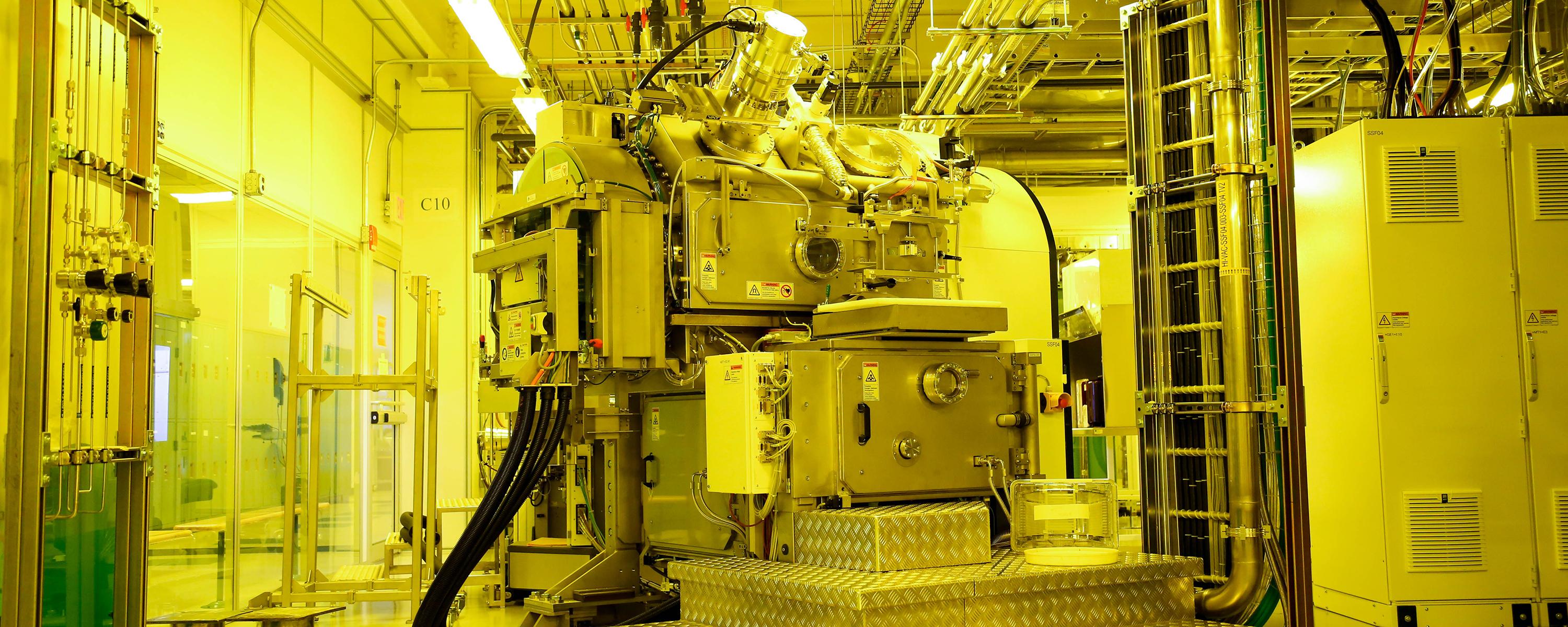
Processing Capabilities
- 100 to 200 mm Substrates
- Silicon, Glass, Ceramic, Polymer - Standard and Custom Processes Supported
- Thin Film Deposition
- Patterning
- Etching
- Bonding
- CMP
- Complete Metrology Suite
For more information on tools, availability, and how to get your project started please contact Ross Goodman at rgoodman@sunypoly.edu