Measurement Methods
Ellipsometry and Scatterometry
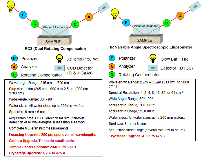
Equipment: Woollam Spectroscopic Ellipsometers – VUV VASE, IR-VASE, RC2
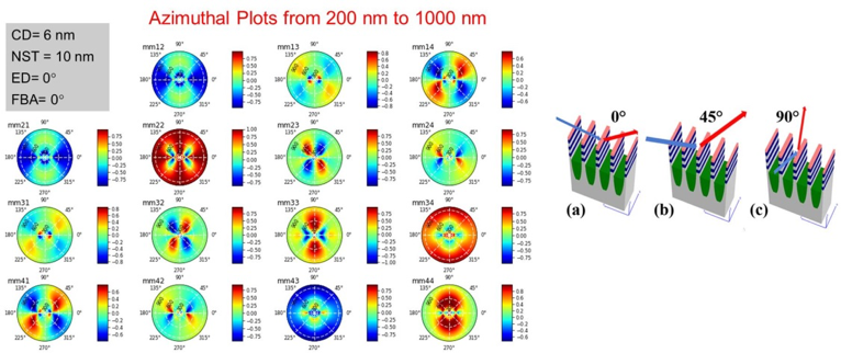
Scatterometry: NanoDiffract (Mueller Matrix) software
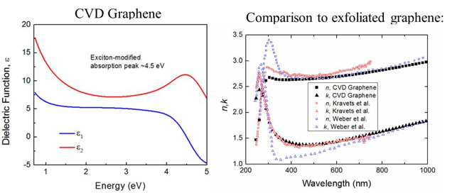
Ellipsometry is a power measurement method capable of determining both film thickness and the dielectric function (complex refractive index) of a material or structure. Optical properties are determined from the change in polarization of elliptically polarized light after reflection from a surface. Spectroscopic ellipsometry has the advantage of measuring optical properties over a range of photon energies. We have laboratory ellipsometers that cover a wide range of wavelengths from 30 microns (Far IR) to 150 nm (VUV). Our in-line ellipsometer covers the range from the near IR to 150 nm in the VUV. The RC2 spectroscopic ellipsometer obtains the complete 16 Mueller Matrix elements vs wavelength.
Using advanced analysis, ellipsometry is capable of measuring the shift in critical points due to quantum confinement of thin semiconductor layers. Ellipsometry provides materials characterization of insulators, semiconductors, and thin metal films. Using advanced software, scatterometry can determine the cross-sectional shape and dimension of lines or contact holes when spectroscopic ellipsometry is used to characterize a grating structure.
The determination of the average shape and dimensions of a lithographically patterned grating structure using Mueller Matrix spectroscopic ellipsometry and a Rigorous Coupled Wave Approximation to solve Maxwell’s equations is known as Scatterometry. (See- Perspective: Optical measurement of feature dimensions and shapes by scatterometry, A.C. Diebold, A. Antonelli, N. Keller, APL Mat. 6, (2018), 058201: abstract: https://doi.org/10.1063/1.50)
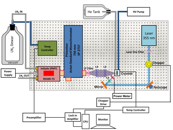
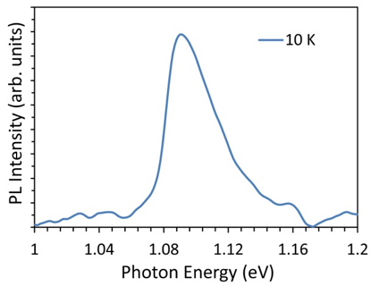
Photoluminescence
Photoluminescence (PL) spectroscopy is a nondestructive optical metrology technique that is used to characterize the electronic structure of materials. The process of absorption of photons of higher energy than the bandgap of the material, and the resulting emission of lower energy photons is the fundamental principle behind PL.i The photo-excitation in the PL measurements was carried out using a 355 nm optically pumped semiconductor laser (OPSL). Circularly polarized light is available for selective excitation of K vs K’ photoluminescence from transition metal dichalcogenides.
i S. Perkowitz, Optical Characterization of Semiconductors: Infrared, Raman, and Photoluminescence Spectroscopy (Academic Press, New York, 1993).
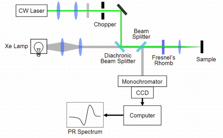
Photoreflectance
Photoreflectance is a modulation spectroscopy used to study the properties of semiconductor surfaces and interfaces. The change in reflectance is measured while the built-in electric field in the material being studied is modulated by a pump laser with photon energy higher than the band gap. Sharp derivative spectral features are presented in the region where optical excitation occurs, even in room temperature. Photoreflectance is sensitive to energy band structures, thus characterizes changes in the critical points* of semiconductors and stress, charge trapping in dielectric layers on semiconductors, and dopant concentrations in III-V materials.
*A critical point is a region along the band structure where a high probability of absorption exists. Critical points are found in the band structure in k-space where the energy separation E between the valence and conduction band is nearly constant. These regions of k-space result in large joint density of states and are referred to as critical points in the Brillouin zone.
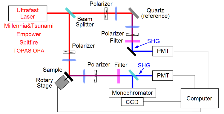
Second Harmonic Generation
Equipment: Newport Spectra-Physics Femto Second Lasers (Tsunami, Spitfire, TOPAS)
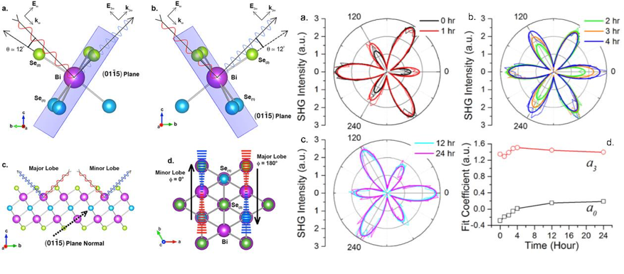
Optical second harmonic generation is a non-linear optical characterization method that is highly sensitive to interfaces and spin states. The second harmonic output (i.e. the photons produced at twice the probe light frequency) is produced by nonlinear optical processes. For example SHG be used to probe the interface between crystalline silicon and a transparent dielectric layer such as interface of Si(111)/SiO2, Si(001)/SiO2 and reconstructed Si(111) and (100) surfaces. The fact that OSG can observe the surface reconstruction effects on the surface symmetry means that OSG is sensitive to the monolayer thick crystal structures.),. The electric field of the light polarizes the electrons in the lattice. For centro-symmetric crystals such as silicon, the bulk polarization is very weak and only occurs in `electric quadrupole’ contributions. However, the surface breaks this symmetry and the stronger surface dipole effect contributes to the observed signal. For non-centro-symmetric crystals such as GaAs, the bulk is more easily polarized and bulk signal will be strong. SHG is also sensitive to the electric field resulting from charge trapped in a surface oxide layer and can be used to observe changes in defect states in HfO2 films. SHG of nano-scale structures is largely unexplored, and the fact that interfaces dominate these structures makes it an important characterization method.
Other Measurement Capability at SUNY Polytechnic Institute
X-ray photoemission spectroscopy (XPS)
Equipment: Thermo-Fisher VG Theta Probe
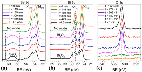
X-ray photoemission spectroscopy (XPS) is a powerful tool for analyzing materials that are used in integrated circuits. XPS can measure both the core levels and the valence band of materials in the near surface (~70-100 Å) region. One of the primary systems we have studied with XPS is the high-k/metal gate stack. In this stack, if the films are thin enough, core levels from each layer can be measured. This allows us to evaluate the chemical composition of each layer, the band alignment between the layers, and the band bending in the substrate. Another material system we have studied is NiSi/Si, which is critical in the electrical contact between the transistor electrodes and the Cu vias. XPS allowed us to distinguish between Ni and NiSi, and to identify the surface oxide associated with each material. XPS has also enabled the study of the time dependence of the oxidation of Topological Insulator Bi2Se3. This work aided in the development of optical models for spectroscopic ellipsometry analysis of these materials.
Advanced Microscopy
Equipment: FEI (ThermoElectron) Titan/ Aberration Corrected STEM/ with EDS and ELS and JEOL 2010F Transmission Electron Microscope (TEM) with EELS
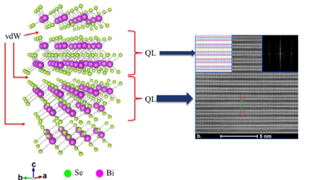
We routinely use advanced microscopy of all types including transmission electron microscopy (TEM), acoustic microscopy, and IR microscopy. Recent advances in TEM have greatly improved image resolution through aberration correction. Of particular interest is scanning TEM (STEM) and electron energy loss analysis. Under optimum conditions, a single atom in an atomic column of a well ordered single crystal can be located using STEM and ELS. We also have a strong interest in high resolution ELS characterization of local chemical bonding at interfaces. The group has MacTempas image simulation software that guides experimental work and aid in image interpretation.
X-ray Metrology
Synchrotron based GI-I-XRD:
Grazing Incidence – In plane- X-Ray Diffraction and Pole Figure Analysis of grain texture is done at Synchrotron facilities such as Brookhaven National Laboratory’s NSLS-II. This capability is sued to determine the crystal phase of ultra-thin high K and metal gate structures.
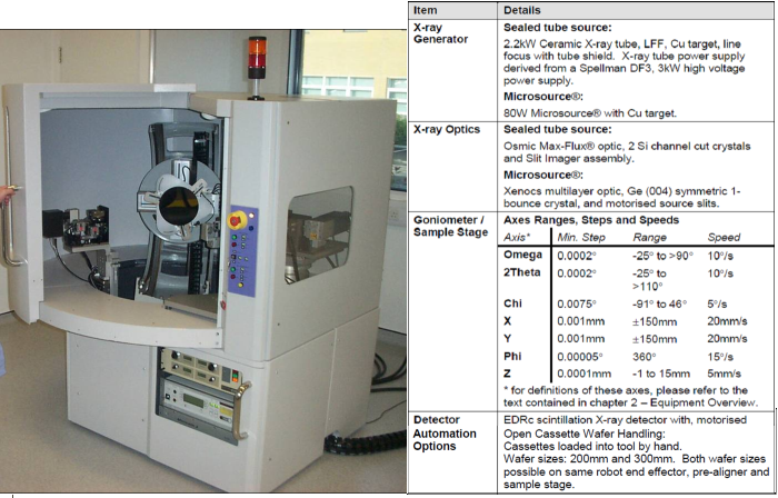
Equipment: BEDE Metrix-L X-Ray Tool
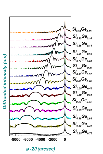
High-Resolution X-Ray Diffraction (HRXRD) : Is used to measure structural parameters in highly perfect materials such as epitaxial layers on single-crystal substrates. Bede RADS software uses full dynamical diffraction theory, the Takagi-Taupin equations, to calculate patterns expected from a given structure.
- Epitaxial structures
- Alloy composition of layers and layer mismatch
- Layer thicknesses
- Relaxation
- Offcut, and tilt between layers and substrate
- Superlattice and MQW period
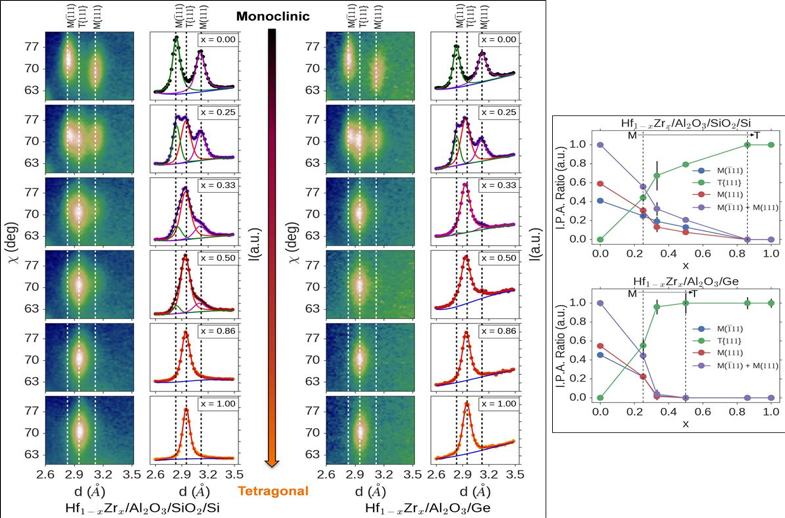
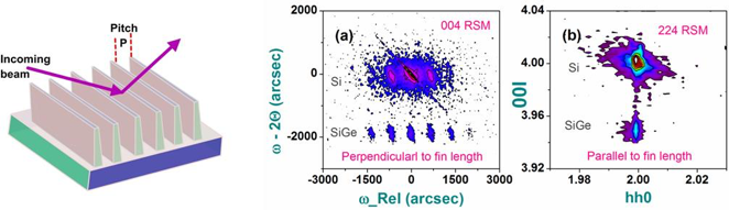
High Resolution Triple Axis Diffraction : A reciprocal space map can be built up by scanning Omega- 2Theta for different offset Omega angles, to give a picture of the complete diffracted intensity distribution about a particular reciprocal lattice point. An Omega scan in triple axis therefore investigates the tilt mosaic at a given d-spacing. An Omega-2Theta scan investigates the variations in strain at a given tilt angle. In double axis HRXRD, both these effects, if present in the sample, are collected in the detector at the same time. Triple axis HRXRD separates them. Current research includes characterization of multilayer Si/SiGe/Si/SiGe/Si/SiGe/Si/SiGe/Si film stacks.
High Resolution X-Ray Reflectivity (HRXRR) : Also known as “grazing incidence X-ray scattering” is a means of measuring layer thickness (less than ~ 500 nm), density and surface and interface roughness (less than ~ 3 nm rms).