Project description
- Extend WBG power semiconductor device research beyond on-wafer characterization by developing power packaging that enables testing of WBG power semiconductor devices at high temperature (150 oC to 300 oC) and high voltage (600 V to 25 kV)
- Collaborate with academia, government, and industry partners on Level-1 to Level-3 power packaging design and packaging material evaluation
Research highlight
- A joint collaboration with Indium Corporation (Clinton, NY), funded by NYS CATN2 MIP, is underway to evaluate advanced packaging materials (die attachment, thermal interface materials, epoxies) in support of the increasing trend to adopt WBG power semiconductor devices in power electronics applications, such as electric vehicle motor drives.
 |
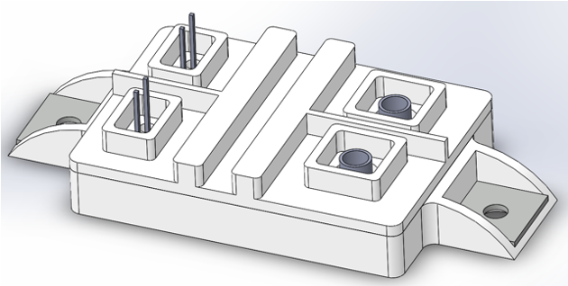 |
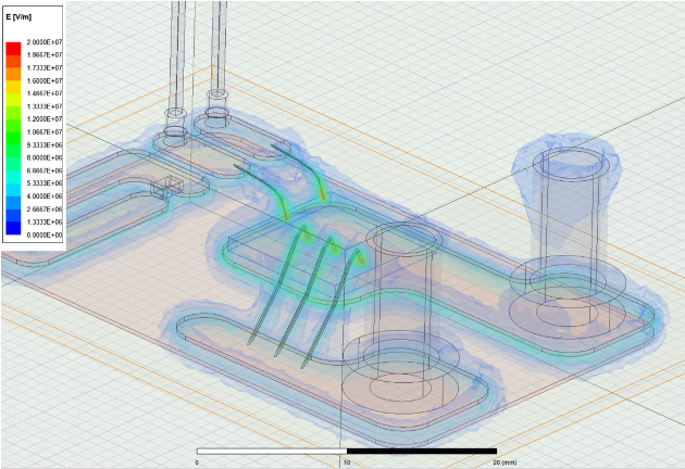
| ANSYS simulation of electric field distribution around packaged power semiconductor device | 3D model of discrete high voltage power package for power semiconductor device testing |